-
- Contact Us
- Privacy Policy
- term and condition
- Cookies policy
MDP16031K00GD04: Latest Specs & TCR Performance Report
The MDP16031K00GD04 is a compact 8-element thick-film resistor network in a 16‑pin DIP with nominal 1 kΩ values and ±2% tolerance. Published figures list a typical TCR of ±100 ppm/°C, an operating range from −55°C to +125°C, per‑element power ≈250 mW, and package footprint roughly 21.6 × 6.35 mm. These numbers determine board-level stability: TCR governs thermal drift, tolerance sets initial accuracy, and per‑element power limits determine derating and layout decisions.
Understanding those specs lets engineers predict gain shift in sensor front-ends, reference divider drift for ADCs, and thermal loading in dense digital arrays. The following report translates the raw numbers into practical selection rules, test procedures, and PCB guidance for US engineering teams.
1 — Product overview: MDP16031K00GD04 at a glance
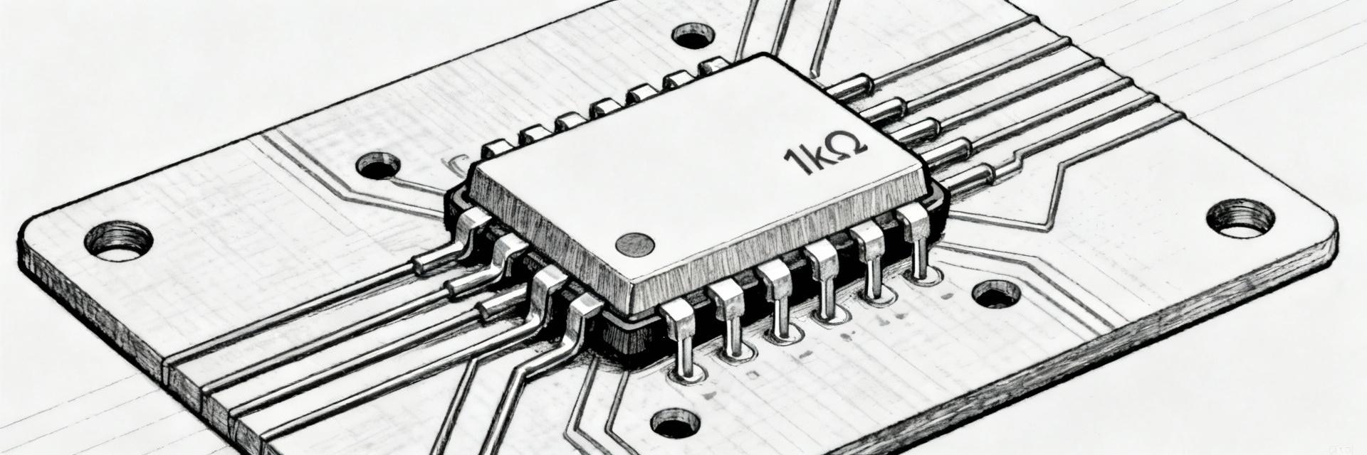
This section summarizes mechanical and electrical attributes that matter for selection and layout. The package is a standard dual‑in‑line network with 16 pins and 2.54 mm pitch. Eight resistors are available in isolated or commonly bussed arrangements; use isolated variants where independent divider legs are required. The nominal resistance is 1 kΩ with ±2% tolerance and per‑element power near 250 mW; these figures set the baseline for thermal and precision calculations.
1.1 — Physical & pinout summary
| Spec | Value |
|---|---|
| Package type | 16‑pin DIP (dual‑in‑line) |
| Pin count / pitch | 16 pins / 2.54 mm |
| Elements | 8 resistors |
| Nominal size (L × W mm) | ~21.6 × 6.35 |
| Seated height | Standard DIP height (dependent on molding) |
| Tolerance | ±2% |
For quick PCB drawing, use the 2.54 mm grid and a 16‑pin footprint with recommended keepouts for thermal relief. Refer to the official datasheet for a pinout diagram and recommended land pattern when preparing production Gerbers.
1.2 — Core electrical specs
Key electrical numbers: 1 kΩ nominal, ±2% tolerance, ~250 mW per element, eight elements per package, and TCR ≈ ±100 ppm/°C. The designation MDP16031K00GD04 is useful when ordering samples or requesting test parts. Choose bussed or isolated variants based on whether a common node is desired; isolated parts avoid interaction between channels in precision divider networks.
2 — TCR performance analysis: what ±100 ppm/°C means in practice
TCR is the temperature coefficient of resistance: it quantifies how much resistance changes per degree. At ±100 ppm/°C, a 1 kΩ resistor changes by 0.1 Ω per °C in the nominal direction indicated by the sign. Translating ppm into absolute change is the most direct way to assess drift impact on circuits.
2.1 — Interpreting TCR for drift and precision
Worked example: for a −40°C → +85°C window (ΔT = 125°C), ΔR = R0 × TCR × ΔT = 1000 Ω × 100×10⁻⁶/°C × 125°C = 12.5 Ω, i.e., 1.25% change. Over the full −55°C → +125°C range (ΔT = 180°C), expect ≈18 Ω or 1.8% change. In sensor front‑ends or ADC references, that magnitude can move gain or offset significantly; designers must budget TCR‑induced ppm drift into system error budgets.
2.2 — Measured vs. spec TCR: test recommendations
To verify TCR, use a temperature chamber or controlled hotplate and a high‑resolution instrument (0.01% or better, e.g., 6½‑digit DMM or bridge). Avoid self‑heating by driving minimal test current and allow thermal stabilization at each setpoint. Plot resistance vs. temperature and compute the slope (ppm/°C) from a linear fit; include error bars and note hysteresis between heating and cooling cycles.
3 — Electrical specs deep-dive: tolerance, power, noise and reliability
Tolerance and power interact with TCR to define both initial accuracy and in‑service stability. ±2% tolerance sets the starting point; combined with TCR‑driven drift, total worst‑case deviation can exceed several percent across wide temperature swings. Designers should apply power derating rules to avoid accelerated drift or failure.
3.1 — Tolerance, power derating and thermal considerations
Derating: treat the ~250 mW per element as a maximum at ambient; apply typical derating so continuous dissipation at high ambient is reduced (common practice: 50% rating at elevated temps). On PCB, provide copper pours for heat spreading and spacing between networks and hot components. Use worst‑case combinations of tolerance and TCR in tolerance stacks when sizing resistors for precision dividers.
3.2 — Noise, long-term drift and failure modes
Thick‑film networks exhibit modest thermal and flicker noise compared with metal‑film types; expect low‑frequency drift over life due to aging. For critical specs, run accelerated aging (biased life) and humidity soak tests. Typical failure modes in field returns are value shifts and opens; include in‑circuit monitoring where possible and design to tolerable fail‑safe margins per the parts' specs.
4 — How to evaluate MDP16031K00GD04 in your design: test & selection checklist
Selection should start with matching application needs to part characteristics: required tolerance, allowable TCR, power per element, number of channels, and footprint constraints. If TCR‑driven drift exceeds system error budget, consider lower‑TCR alternatives or temperature compensation strategies.
4.1 — Pre-selection checklist (spec vs. application)
- Tolerance target: is ±2% acceptable or is ±0.1% needed?
- TCR target: is ±100 ppm/°C within your drift budget?
- Power: confirm per‑element dissipation and derating needs.
- Footprint: 16‑pin DIP fit and board area vs. space constraints.
- Topology: isolated vs. bussed — pick per circuit isolation needs.
4.2 — Recommended validation tests (lab & in-circuit)
Run temperature sweep tests with low measurement current, power‑cycling under bias, thermal cycling per intended environment, and humidity soak. For in‑circuit checks, monitor divider outputs across thermal ramps and compare to bench measurements. Establish pass/fail thresholds tied to ADC LSB or system gain tolerances.
5 — Application examples and PCB layout tips (case study style)
Two anonymous examples illustrate typical tradeoffs. Example A: a sensor front‑end uses matched resistor legs; here TCR and tolerance directly affect gain stability, so match network channels and place away from heat sources. Example B: pull‑up arrays for digital lines care more about power and tolerance than small TCR‑drift, making this network an economical fit.
5.1 — Typical use cases
- Precision divider in low‑gain amplifiers — match channels and validate drift. Watch thermal gradients between resistors.
- Digital pull‑ups / terminators — prioritize power handling and layout to prevent hot spots; TCR less critical.
5.2 — PCB placement and soldering notes
Place networks away from power regulators and hot ICs, use thermal reliefs to avoid localized heat, and provide copper pours for even dissipation. Follow standard reflow profiles and avoid excessive mechanical stress during wave or hand soldering; validate solder profile with sample parts under expected assembly conditions.
6 — Selection & implementation action plan
Use a short matrix to decide fit: if precision budget allows ~1% drift over operating range, this network is acceptable; if sub‑0.1% drift is required, select lower‑TCR options. Always order samples for lab validation and include verified test data in design reviews.
6.1 — Quick selection guide (yes/no matrix)
| Requirement | Fit? |
|---|---|
| Low volume digital pull‑ups | Yes |
| Precision ADC reference divider (sub‑0.1%) | No — choose low‑TCR options |
| Moderate precision sensor arrays | Conditional — match channels and validate |
6.2 — Next steps & documentation to collect
Collect the datasheet, request sample lots for environmental and life testing, perform vendor‑independent TCR verification, and document results in design reviews. Use the part designation MDP16031K00GD04 on procurement and test records to avoid mix-ups.
Summary
- MDP16031K00GD04 is an 8‑element 16‑pin DIP network with 1 kΩ nominal, ±2% tolerance, ~250 mW per element, and a typical TCR of ±100 ppm/°C—suitable for many mixed‑signal board roles but requiring validation for precision use.
- TCR of ±100 ppm/°C yields ≈0.1 Ω/°C (≈12.5 Ω over −40→+85°C); quantify this drift against ADC or sensor error budgets before selection.
- Run chamber sweeps, low‑current resistance measurements, and biased life tests; apply PCB thermal management and derating to ensure reliability under the stated specs.
Frequently Asked Questions
What is the expected resistance change due to TCR for MDP16031K00GD04?
With a nominal 1 kΩ and TCR ≈ ±100 ppm/°C, expect ~0.1 Ω change per °C. Over a 125°C swing (−40→+85°C), that is ~12.5 Ω (~1.25%). Use this figure when budgeting system drift for precision dividers or references.
How should I measure TCR reliably for this resistor network?
Use a temperature chamber or hotplate, a high‑resolution DMM or bridge (better than 0.01%), and minimal test current to avoid self‑heating. Allow thermal stabilization at each setpoint, measure during both heating and cooling, and fit resistance vs. temperature to extract ppm/°C.
Are these networks suitable for ADC reference dividers?
They can be used if the combined tolerance plus TCR‑induced drift stays within the ADC reference stability requirement. For high‑precision ADCs (sub‑100 ppm), choose lower‑TCR and tighter‑tolerance parts or add temperature compensation; for less demanding systems, these networks are an economical choice.
- Technical Features of PMIC DC-DC Switching Regulator TPS54202DDCR
- STM32F030K6T6: A High-Performance Core Component for Embedded Systems
- APT50GH120B Datasheet Deep Dive: Specs, Ratings & Curves
- APT50GH120BSC20 Power Module: Latest Performance Report
- APT50GH120BD30 IGBT: How to Maximize Efficiency for EV Drive
- GTSM20N065: Latest 650V IGBT Test Report & Metrics
- CMSG120N013MDG Performance Report: Efficiency & Losses
- GTSM40N065D Technical Deep Dive: 650V IGBT + SiC SBD
- NOMC110-410UF SO-16: Live Stock & Price Report
- TOMC16031000FT5 Datasheet: Key Specs & Performance
-
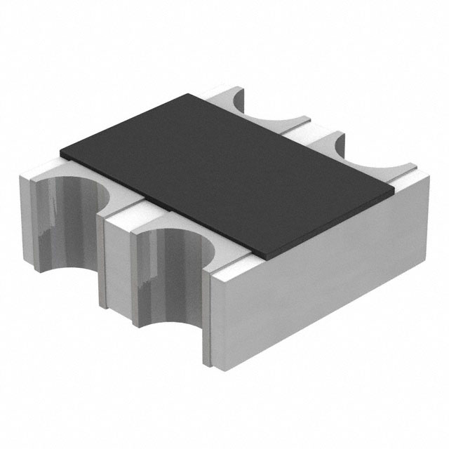 EXB-V4V120JVPanasonic Electronic ComponentsRES ARRAY 2 RES 12 OHM 0606
 -
 EXB-V4V473JVPanasonic Electronic ComponentsRES ARRAY 2 RES 47K OHM 0606
 -
 EXB-V4V823JVPanasonic Electronic ComponentsRES ARRAY 2 RES 82K OHM 0606
 -
 EXB-V4V151JVPanasonic Electronic ComponentsRES ARRAY 2 RES 150 OHM 0606
 -
 EXB-V4V181JVPanasonic Electronic ComponentsRES ARRAY 2 RES 180 OHM 0606
 -
 EXB-V4V331JVPanasonic Electronic ComponentsRES ARRAY 2 RES 330 OHM 0606
 -
 EXB-V4V152JVPanasonic Electronic ComponentsRES ARRAY 2 RES 1.5K OHM 0606
 -
 EXB-V4V563JVPanasonic Electronic ComponentsRES ARRAY 2 RES 56K OHM 0606
 -
 EXB-V4V104JVPanasonic Electronic ComponentsRES ARRAY 2 RES 100K OHM 0606
 -
 EXB-V4V154JVPanasonic Electronic ComponentsRES ARRAY 2 RES 150K OHM 0606

