-
- Contact Us
- Privacy Policy
- term and condition
- Cookies policy

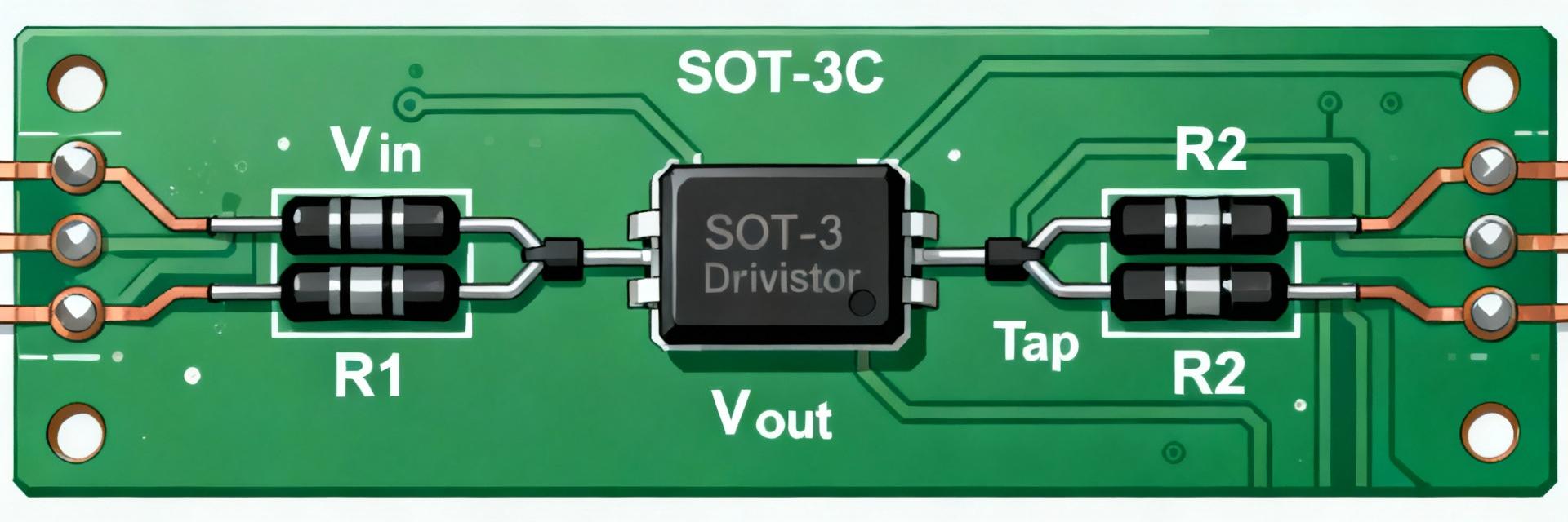
MPMT1002AT5: Complete SOT-23 Divider Specs & Data Sheet
>60% of precision ADC front-end designs use matched thin-film resistor networks in SOT‑23 packages for low-drift scaling and improved CMRR. This note delivers a concise, actionable breakdown of the MPMT1002AT5: what it is, key electrical and mechanical specs, PCB integration tips, application examples, sourcing guidance and where to verify parameters in the official datasheet. The goal is an engineer-ready reference for using this SOT-23 divider in precision front-ends.
The MPMT1002AT5 is presented here as a compact, fixed matched thin‑film resistor network in a SOT‑23 divider footprint. Engineers should consult the official datasheet for authoritative pinout, absolute max ratings and mechanical drawings before design signoff; this article emphasizes practical interpretation and design-impact guidance for quick integration.
1 — What the MPMT1002AT5 Is: Part Overview (Background)
1.1 — Package & Basic Function
The device is a matched thin‑film resistor divider in a SOT‑23 package intended to provide a fixed, accurate resistance ratio for voltage scaling. As a two‑resistor-divider topology it presents a single divided output pin and two end pins; the manufacturer datasheet contains the authoritative pinout and electrical tables. Functionally the part replaces discrete resistor pairs to improve ratio matching, reduce PCB area and lower trimming effort.
1.2 — Typical Applications
Common uses include ADC input scaling, reference/bias networks, op‑amp gain setting and sensor linearization. Example: replacing a discrete 10:1 divider with a matched network reduces systematic ratio error and long‑term drift in precision ADC front‑ends, improving total error budget when amplifier input bias currents and source impedance are managed per the datasheet guidance.
2 — Electrical Specifications (Data Deep‑Dive)
2.1 — Resistance Values, Ratio Tolerance & Tracking
Nominal resistance values and absolute tolerances vary by ordering code; consult the datasheet for the exact nominal set for the chosen device. Ratio tolerance (matching) is the key spec for divider accuracy: for a divider with nominal ratio Rb/(Ra+Rb), small mismatch Δ yields output error approximately Δ_ratio ≈ ΔR / (Ra+Rb) in fractional terms. Designers should use the datasheet ratio tolerance to compute ppm or percentage contribution to the ADC error budget.
2.2 — Temperature Coefficient, Power & Operating Ranges
TCR tracking, operating temperature range and voltage/power limits set the drift and safe‑operating envelope. Typical datasheet entries include TCR (ppm/°C) for absolute and tracking, rated ambient range and maximum continuous voltage. Below is a compact spec summary and design impact; use the datasheet for exact numeric fields for your lot.
| Spec | Typical Value (see datasheet) | Design Impact |
|---|---|---|
| TCR (tracking) | Low ppm/°C | Controls differential drift; critical for long‑term ADC scale stability |
| Operating temp | Industrial range | Derate power and expect additional drift near extremes |
| Max differential voltage / power | Per datasheet | Limits divider placement in high‑voltage front ends; requires derating |
3 — Mechanical, Pinout & PCB Integration (Data + Guide)
3.1 — SOT‑23 Dimensions, Pinout & Footprint
The SOT‑23 divider package offers a compact L×W×H profile with manufacturer mechanical drawing specifying pad land pattern and pin numbering. Follow the datasheet land pattern recommendation for pad size, solder mask clearance and paste mask apertures. A correct footprint prevents tombstoning and ensures solder fillet consistency for this SOT‑23 divider.
3.2 — Thermal and Mounting Considerations
Thermal dissipation is constrained by small package thermal resistance and PCB copper area. Use thermal pours tied to the ground plane, keep trace widths sufficient for power dissipation and avoid placing high‑power components adjacent to the divider. Adhere to the manufacturer reflow profile for peak temperature and dwell times; include the datasheet mechanical drawing in your CAD library filename for traceability.
4 — Application Examples & Design Tips (Method / How‑to)
4.1 — Common Circuit Examples (ADC scaling, Bias networks)
ADC scaling example: for a required scale factor of 0.1, select a divider ratio Rb/(Ra+Rb)=0.1. If Ra and Rb are internal matched elements, total error ≈ ratio_tolerance + TCR-induced drift. Calculate expected Vout = Vin×Rb/(Ra+Rb) and propagate resistor ratio tolerance into ADC LSB error. For op‑amp biasing, use the network to set precise mid‑rail references while minimizing added noise and source impedance.
4.2 — Troubleshooting & Best Practices
Minimize noise by using short traces, guard routing for high‑impedance nodes, and proper bypassing near ADC inputs. Avoid loading the divider with low impedance inputs unless buffered. To validate ratio and TCR on the bench, measure Vout vs Vin across temperature steps and compute fractional deviation against the datasheet ratio tolerance; log results to confirm part lot performance.
5 — Sourcing, Cross‑References & Compliance (Case & Action)
5.1 — Where to Buy, Part Marking & Ordering Options
Purchase through authorized electronics distributors and the manufacturer's sales channels; search the exact part number string and check reel vs. cut‑tape packaging and minimum order quantities. BOM tips: include full ordering code with tolerance and packaging suffix, request reel quantities for production, and document part marking and footprint filename in the BOM comment field to avoid mis‑picks.
5.2 — Equivalent Parts, Cross‑References & Compliance
When seeking equivalents, match ratio tolerance, TCR tracking and package type first, then confirm thermal and voltage limits. Verify RoHS/REACH declarations and any required industrial or automotive qualifications in supplier compliance documents. Always cross‑check electrical tables in the official datasheet before substituting alternate family parts.
Summary
- The MPMT1002AT5 is a compact matched thin‑film SOT‑23 divider that replaces discrete resistor pairs to improve ratio accuracy and drift performance; consult the official datasheet to confirm nominal resistances and pinout for your specific ordering code.
- Key design drivers are ratio tolerance, TCR tracking and maximum voltage/power limits; these determine error budget contribution and placement/thermal strategy on the PCB.
- For reliable integration, add the mechanical drawing and recommended land pattern to the CAD library, follow the reflow profile, and validate divider ratio and drift on the bench before production.
Frequently Asked Questions
What are the nominal resistance values and tolerances for MPMT1002AT5?
Nominal values and absolute tolerances depend on the specific ordering code; consult the official datasheet for the exact resistor values, absolute tolerance and ratio tolerance for the device variant you plan to use. Use those figures to compute the divider's contribution to system gain error and the ADC error budget.
How does the SOT‑23 divider TCR affect ADC scaling stability?
TCR tracking defines how matched resistors change relative to each other with temperature. Even if absolute TCR is modest, close tracking reduces differential drift; compute expected drift contribution by multiplying TCR tracking (ppm/°C) by the anticipated ambient swing and convert to output voltage change relative to Vin.
What PCB footprint and reflow precautions are recommended for MPMT1002AT5?
Use the manufacturer land pattern and solder‑paste aperture recommendations from the datasheet, maintain recommended solder mask clearances, and follow the published reflow profile to avoid tombstoning or excessive stress. Include thermal copper pours if power dissipation approaches datasheet limits and validate solder joints in the first assembly run.
-
 MSP08A0110K0GDA Datasheet & Specs: Complete Quick Report2026-01-02 12:45:27 0Hook — The MSP08A0110K0GDA is commonly listed as a 7-element bussed resistor network in an 8‑pin SIP with a typical nominal resistance of 10 kΩ and published temperature coefficients often near 100 ppm/°C; designers should confirm exact values in the official datasheet before final selection. This quick report summarizes datasheet items and practical implications for engineering and purchasing decisions. Purpose — This fast reference condenses the MSP08A0110K0GDA datasheet essentials and specs so engineers and procurement teams can rapidly evaluate fit, design-in risks, and substitute candidates. It prioritizes electrical limits, mechanical footprint, test guidance, and sourcing checks needed to move from datasheet reading to BOM inclusion. 1 — Quick ID & Overview (background introduction) 1.1 — Part summary and common variants PointThe MSP08A0110K0GDA is a molded single‑in‑line package housing seven resistive elements arranged in a bussed topology; datasheet excerpts report 8 pins, matched elements, and options for tolerance and TCR. EvidenceTypical listings show 10 kΩ nominal and tolerance options; variants trade tolerance or power rating for size. ExplanationChoose the exact suffix when tolerance, power per element, or TCR drive the design. 1.2 — Typical applications PointCommon uses leverage the compact, matched, bussed format. EvidenceEngineers use these arrays where space, matching, and multiple pull resistors are required. ExplanationTypical uses includePull‑up/pull‑down resistor arrays for logic rails — compact matched values and simplified routing. Bus termination in low‑speed lines — bussed common simplifies multi‑line terminations. Sensor interface resistor networks — matched elements reduce offset and drift between channels. Compact, space‑constrained PCBs — SIP footprint packs multiple resistors in one component. 2 — Complete Electrical Specs & Ratings (data analysis) 2.1 — Key electrical parameters to extract from the datasheet PointA checklist ensures no critical spec is missed. EvidenceDatasheets list resistance, tolerance, TCR, power per element, max working voltage, insulation/resistance to substrate, and operating temperature range. ExplanationBefore approval, pull exact numeric values for each item and flag discrepancies across distributor listings and revisions. Resistance value(s) and configuration (bussed vs isolated) Tolerance classes (%), available options Temperature coefficient (ppm/°C) Power dissipation per element (mW or W) and derating rules Maximum working/continuous voltage and insulation to substrate Operating temperature range and storage limits 2.2 — Typical performance examples & how to interpret them PointTranslate TCR and tolerance into expected in‑circuit behavior. EvidenceFor a 10 kΩ element with 100 ppm/°C over −40 to +85 °C (ΔT = 125 °C), the fractional change is 0.0125, i.e., ~1.25% drift or ~125 Ω. ExplanationUse this to budget worst‑case drift; similarly compute power using P = V²/R to check element limits in bussed versus isolated wiring. 3 — Pinout, Package & Mechanical Data (data analysis / method) 3.1 — Pin numbering, circuit diagram & footprint notes PointAccurate pin documentation prevents assembly errors. EvidenceThe datasheet figure defines which pins form the common bus and which are individual terminals; footprints use standard SIP pitch. ExplanationRecreate the datasheet diagram in CAD, verify pin pitch and body length, and include a silkscreen reference; avoid guessing common pin location — confirm from the official drawing. 3.2 — Mechanical, thermal and packaging details to verify PointMechanical checks affect PCB yield and thermal behavior. EvidenceImportant specs include package length/width/height, lead finish, recommended land pattern, and packaging type (tube or reel). ExplanationVerify lead finish for solderability, follow recommended land pattern, and apply thermal derating if the per‑element power is limited by package heat sinking. 4 — Design, Testing & Integration Guidance (method / practical) 4.1 — Design checklist for engineers PointA short integration checklist reduces rework. EvidenceActions to take include confirming electrical ratings, checking power dissipation per element, planning thermal reliefs, and specifying tolerance in the BOM. ExplanationExample — if a termination sees 5 V across 10 kΩ, P = V²/R = 2.5 mW; this is well below common per‑element ratings, but parallel or bussed uses can concentrate power and require derating. 4.2 — Test and validation recommendations PointPractical tests catch subtle failures early. EvidenceRecommended bench tests include room‑temperature resistance verification, controlled temperature sweeps to measure drift, power cycling, and long‑term drift characterization for matched networks. ExplanationWatch for common failure modes such as element overpower, solder fatigue, and package cracking; document test conditions to match intended field use. 5 — Sourcing, Cross-References & BOM Tips (case study / action) 5.1 — How to verify you have the correct datasheet and part variant PointFull part‑number matching avoids costly mistakes. EvidenceConfirm the complete PN suffix, package type, element count/configuration, resistance value, tolerance, and power rating against the datasheet revision. ExplanationUse a long‑tail search phrase such as "MSP08A0110K0GDA resistor network datasheet download" to locate the official datasheet PDF and compare pin count and dimensional drawing before ordering. 5.2 — Alternatives, substitutions & procurement tips PointSubstitutes must match electrical and mechanical constraints. EvidenceMatch package, element count and topology (bussed vs isolated), resistance/tolerance, TCR and power per element; also check MOQ, lead time, packaging, and lifecycle status. ExplanationCreate a procurement checklist that includes lifecycle status and packaging type to avoid end‑of‑life surprises and requalification work. Summary (conclusion & quick-spec snapshot) Recap — The MSP08A0110K0GDA is typically a 7‑element, 8‑pin bussed resistor network with a common nominal value near 10 kΩ; designers must confirm the exact variant and datasheet revision before final selection. Three critical checks are power per element, TCR (ppm/°C) and package/footprint to ensure thermal and assembly compatibility. Download the datasheet and run the checklist prior to BOM freeze. MSP08A0110K0GDA typical identity8‑pin SIP, 7 bussed resistors, ~10 kΩ nominal; verify in datasheet. Electrical prioritiesconfirm tolerance, TCR (ppm/°C), power per element and max working voltage before design signoff. Mechanical prioritiesconfirm pin pitch, body length, lead finish and recommended land pattern to reduce PCB rework. 5 — 常见问题解答 (FAQ) What are the MSP08A0110K0GDA datasheet key electrical ratings? Answer — Key electrical ratings to extract from the datasheet include each element's nominal resistance, tolerance class, temperature coefficient in ppm/°C, power dissipation per element, maximum working voltage, insulation resistance to substrate, and operating temperature range. Verify these against the exact part suffix and datasheet revision before approving the component for production. How should MSP08A0110K0GDA specs be interpreted for temperature drift? Answer — Use the TCR value to compute worst‑case driftfractional change = TCR(ppm/°C) × ΔT. For example, 100 ppm/°C over a 125 °C range yields ~1.25% change; for a 10 kΩ part this equals ~125 Ω shift. Budget this drift into accuracy margins and matching requirements. What are acceptable substitutes for MSP08A0110K0GDA resistor network? Answer — Acceptable substitutes must match topology (bussed vs isolated), element count, package (8‑SIP footprint), resistance and tolerance, TCR, and per‑element power. Also check footprint compatibility and thermal behavior; if any spec differs, re‑evaluate in‑circuit heating and matching implications before substituting on a production BOM.READ MORE
 -
 HEIKIT1020050E29 Stock, Specs & US Sourcing Report2026-01-01 12:35:48 0Aggregate distributor snapshots and recent channel checks show variable availability for HEIKIT1020050E29 — inventory reports range from single-digit quantities to low hundreds, with factory lead times reported up to ~10 weeks. This volatility makes timely, specs-verified sourcing critical for US buyers who need predictable supply and validated mechanical fit. The purpose of this report is to summarize the current stock landscape, list the technical specs to verify before purchase, outline practical US sourcing routes, and provide an immediate procurement checklist so teams can act quickly and reduce risk when buying this part. 1 — Product snapshot: what HEIKIT1020050E29 is and why it matters (background) — Part overview & typical applications HEIKIT1020050E29 is a piece of resistor mounting hardware designed for thru-bolt horizontal mounting of high-power resistors. The item typically includes a metal bracket and associated mounting hardware sized for specific resistor footprints; intended uses include power electronics assemblies, test racks, and heavy-current distribution modules. Correct part selection matters because improper bracketry or incorrect hole spacing leads to assembly rework, poor thermal contact, and field failures. — Key identifiers & ordering details to confirm Before purchasing, confirm the full part number and any suffixes, packaging codes, footprint orientation (horizontal vs. vertical), and mounting hole spacing. Compare supplier listing identifiers against the authoritative datasheet: matching mechanical drawings, ordering codes, and optional finishes. Always quote the exact ordering code on the PO and request the supplier to confirm the datasheet revision and packaging quantity before allocation. 2 — Current US stock landscape & pricing signals (data analysis) — Inventory snapshot across US channels Observed inventory across US channels varies: some sellers report single-digit stock, others low-hundreds, and some listings show out-of-stock with incoming allocations. Interpret channel quantities carefully — allocated stock, consignment, and broker holdings look similar on a snapshot but have different fulfillment risk. Conduct live stock checks across multiple sources and record the timestamped results to avoid surprises during PO acceptance. — Lead times, price volatility & availability trends Lead times trend in two bands: immediate ship for in-channel stock and factory lead times that can extend to approximately ten weeks. Price volatility often increases when on-hand stock is low; broker premiums and rush fees can raise unit cost substantially. Monitor changes daily if the part is critical; use RFQs with firm quotes and set alerts to capture sudden price moves or new supply introductions. Live-stock snapshot (example): observed channel availability ranges from 5–250 units; several listings marked as allocated or consignment; reported factory lead times up to ~10 weeks. Treat this as a planning snapshot and confirm live counts before PO issuance. 3 — Technical specifications & interchange guidance (data/specs) — Must-check technical specs before buying Checklist: verify mechanical dimensions and mounting hole spacing against PCB or chassis drawings; confirm bracket material and finish (corrosion resistance and conductivity); validate maximum working temperatures and mechanical load ratings; and check any electrical ratings if part contacts conductive elements. Watch for ambiguous drawings and optional finishes; always quote exact datasheet values and request dimensional drawings where tolerances impact fit. — Cross-reference & substitution strategy To identify compatible alternatives, match footprint, mounting style, hole spacing, and material/finish. Substitution rules: never compromise hole spacing or thickness that affects structural strength; optional surface finishes may be acceptable if electrical and corrosion performance are equivalent. Document any interchange decision: list original vs. substitute part numbers, justification, test or sample validation, and an approval record in procurement files. 4 — US sourcing playbook: where to buy and how to reduce risk (method guide) — Buying routes & cost drivers Typical sourcing options include authorized distributor stock, broadline channel distributors, independent brokers, and direct factory specials. Cost drivers are MOQ, packaging type, rush fees, broker premiums, and obsolescence risk. For HEIKIT1020050E29 prioritize authorized inventory for traceability when possible, but factor broker supply for short-term needs while accounting for higher unit cost and verification steps to confirm authenticity and specs. — Procurement process & negotiation tactics Step-by-step: verify specs against the datasheet → request up-to-date stock confirmation with timestamps → request photos or sample verification showing part marking and packaging → secure allocation with PO terms or deposit → confirm lead times and penalties for missed dates. Negotiate staged deliveries, partial allocations, and firm lead-time commitments; use sample orders for physical fit checks before large releases. 5 — Alternatives, lifecycle signals & immediate action checklist (case + action) — When to choose an alternative part — quick selection criteria Choose an alternative when it offers materially faster lead time, a meaningful price advantage, or identical mounting and strength characteristics. Watch lifecycle signals: sudden disappearance from multiple channels, repeated "last-time buy" notices, or supplier end-of-life bulletins. If lifecycle signals appear, plan a redesign or last-time buy depending on production horizon and risk tolerance. — 5-step immediate actions for US procurement teams Quick checklist: 1) Confirm live stock counts and dates across channels, 2) download and compare datasheet specs, 3) request sample or photo verification, 4) lock allocation with PO or deposit, 5) plan safety stock for critical runs. RFQ email template line: "Please confirm live stock (quantity/date), datasheet revision, and shipment ETA for full part number." PO note sample: "Confirm datasheet values and lead-time; ship per agreed schedule; penalties apply for late delivery." Summary HEIKIT1020050E29 requires datasheet verification and live stock checks; availability ranges from immediate shipments to factory lead times near ten weeks, so confirm timestamped inventory before PO. Verify critical specs—mounting hole spacing, bracket material/finish, and mechanical ratings—and document any substitution with test evidence and procurement approvals. Use a mixed sourcing strategy: prefer authorized stock for traceability, use brokers for short-term fills, and apply staged delivery and allocation tactics to reduce supply risk. Frequently Asked Questions How should procurement confirm reported stock quantities? Confirm reported stock by requesting a timestamped stock confirmation and photos of the physical packaging showing part markings and quantity. Record the seller contact, the time of confirmation, and any allocation notes. Where possible, ask for an available-to-promise (ATP) date and get that in writing on the PO to reduce fulfillment risk. What are the most common datasheet pitfalls to avoid? Pitfalls include ambiguous mechanical drawings without clear tolerances, optional finish variants that change corrosion resistance, and unclear packaging quantities. Always quote exact datasheet values, request dimensional drawings when fit is critical, and confirm the finish specified on the supplier invoice matches the datasheet option you specified. When is it justified to pay a broker premium for immediate stock? Pay a broker premium when production cannot be interrupted, the premium is smaller than the cost of line downtime, and you have verified part authenticity and specs. Require stamped photos, shipment proof, and a limited warranty or return clause; use premium purchases sparingly and document the business justification for audit trails.READ MORE
 -
 MDP16031K00GD04: Latest Specs & TCR Performance Report2025-12-30 12:47:56 0The MDP16031K00GD04 is a compact 8-element thick-film resistor network in a 16‑pin DIP with nominal 1 kΩ values and ±2% tolerance. Published figures list a typical TCR of ±100 ppm/°C, an operating range from −55°C to +125°C, per‑element power ≈250 mW, and package footprint roughly 21.6 × 6.35 mm. These numbers determine board-level stabilityTCR governs thermal drift, tolerance sets initial accuracy, and per‑element power limits determine derating and layout decisions. Understanding those specs lets engineers predict gain shift in sensor front-ends, reference divider drift for ADCs, and thermal loading in dense digital arrays. The following report translates the raw numbers into practical selection rules, test procedures, and PCB guidance for US engineering teams. 1 — Product overviewMDP16031K00GD04 at a glance This section summarizes mechanical and electrical attributes that matter for selection and layout. The package is a standard dual‑in‑line network with 16 pins and 2.54 mm pitch. Eight resistors are available in isolated or commonly bussed arrangements; use isolated variants where independent divider legs are required. The nominal resistance is 1 kΩ with ±2% tolerance and per‑element power near 250 mW; these figures set the baseline for thermal and precision calculations. 1.1 — Physical & pinout summary SpecValue Package type16‑pin DIP (dual‑in‑line) Pin count / pitch16 pins / 2.54 mm Elements8 resistors Nominal size (L × W mm)~21.6 × 6.35 Seated heightStandard DIP height (dependent on molding) Tolerance±2% For quick PCB drawing, use the 2.54 mm grid and a 16‑pin footprint with recommended keepouts for thermal relief. Refer to the official datasheet for a pinout diagram and recommended land pattern when preparing production Gerbers. 1.2 — Core electrical specs Key electrical numbers1 kΩ nominal, ±2% tolerance, ~250 mW per element, eight elements per package, and TCR ≈ ±100 ppm/°C. The designation MDP16031K00GD04 is useful when ordering samples or requesting test parts. Choose bussed or isolated variants based on whether a common node is desired; isolated parts avoid interaction between channels in precision divider networks. 2 — TCR performance analysiswhat ±100 ppm/°C means in practice TCR is the temperature coefficient of resistanceit quantifies how much resistance changes per degree. At ±100 ppm/°C, a 1 kΩ resistor changes by 0.1 Ω per °C in the nominal direction indicated by the sign. Translating ppm into absolute change is the most direct way to assess drift impact on circuits. 2.1 — Interpreting TCR for drift and precision Worked examplefor a −40°C → +85°C window (ΔT = 125°C), ΔR = R0 × TCR × ΔT = 1000 Ω × 100×10⁻⁶/°C × 125°C = 12.5 Ω, i.e., 1.25% change. Over the full −55°C → +125°C range (ΔT = 180°C), expect ≈18 Ω or 1.8% change. In sensor front‑ends or ADC references, that magnitude can move gain or offset significantly; designers must budget TCR‑induced ppm drift into system error budgets. 2.2 — Measured vs. spec TCRtest recommendations To verify TCR, use a temperature chamber or controlled hotplate and a high‑resolution instrument (0.01% or better, e.g., 6½‑digit DMM or bridge). Avoid self‑heating by driving minimal test current and allow thermal stabilization at each setpoint. Plot resistance vs. temperature and compute the slope (ppm/°C) from a linear fit; include error bars and note hysteresis between heating and cooling cycles. 3 — Electrical specs deep-divetolerance, power, noise and reliability Tolerance and power interact with TCR to define both initial accuracy and in‑service stability. ±2% tolerance sets the starting point; combined with TCR‑driven drift, total worst‑case deviation can exceed several percent across wide temperature swings. Designers should apply power derating rules to avoid accelerated drift or failure. 3.1 — Tolerance, power derating and thermal considerations Deratingtreat the ~250 mW per element as a maximum at ambient; apply typical derating so continuous dissipation at high ambient is reduced (common practice50% rating at elevated temps). On PCB, provide copper pours for heat spreading and spacing between networks and hot components. Use worst‑case combinations of tolerance and TCR in tolerance stacks when sizing resistors for precision dividers. 3.2 — Noise, long-term drift and failure modes Thick‑film networks exhibit modest thermal and flicker noise compared with metal‑film types; expect low‑frequency drift over life due to aging. For critical specs, run accelerated aging (biased life) and humidity soak tests. Typical failure modes in field returns are value shifts and opens; include in‑circuit monitoring where possible and design to tolerable fail‑safe margins per the parts' specs. 4 — How to evaluate MDP16031K00GD04 in your designtest & selection checklist Selection should start with matching application needs to part characteristicsrequired tolerance, allowable TCR, power per element, number of channels, and footprint constraints. If TCR‑driven drift exceeds system error budget, consider lower‑TCR alternatives or temperature compensation strategies. 4.1 — Pre-selection checklist (spec vs. application) Tolerance targetis ±2% acceptable or is ±0.1% needed? TCR targetis ±100 ppm/°C within your drift budget? Powerconfirm per‑element dissipation and derating needs. Footprint16‑pin DIP fit and board area vs. space constraints. Topologyisolated vs. bussed — pick per circuit isolation needs. 4.2 — Recommended validation tests (lab & in-circuit) Run temperature sweep tests with low measurement current, power‑cycling under bias, thermal cycling per intended environment, and humidity soak. For in‑circuit checks, monitor divider outputs across thermal ramps and compare to bench measurements. Establish pass/fail thresholds tied to ADC LSB or system gain tolerances. 5 — Application examples and PCB layout tips (case study style) Two anonymous examples illustrate typical tradeoffs. Example Aa sensor front‑end uses matched resistor legs; here TCR and tolerance directly affect gain stability, so match network channels and place away from heat sources. Example Bpull‑up arrays for digital lines care more about power and tolerance than small TCR‑drift, making this network an economical fit. 5.1 — Typical use cases Precision divider in low‑gain amplifiers — match channels and validate drift. Watch thermal gradients between resistors. Digital pull‑ups / terminators — prioritize power handling and layout to prevent hot spots; TCR less critical. 5.2 — PCB placement and soldering notes Place networks away from power regulators and hot ICs, use thermal reliefs to avoid localized heat, and provide copper pours for even dissipation. Follow standard reflow profiles and avoid excessive mechanical stress during wave or hand soldering; validate solder profile with sample parts under expected assembly conditions. 6 — Selection & implementation action plan Use a short matrix to decide fitif precision budget allows ~1% drift over operating range, this network is acceptable; if sub‑0.1% drift is required, select lower‑TCR options. Always order samples for lab validation and include verified test data in design reviews. 6.1 — Quick selection guide (yes/no matrix) RequirementFit? Low volume digital pull‑upsYes Precision ADC reference divider (sub‑0.1%)No — choose low‑TCR options Moderate precision sensor arraysConditional — match channels and validate 6.2 — Next steps & documentation to collect Collect the datasheet, request sample lots for environmental and life testing, perform vendor‑independent TCR verification, and document results in design reviews. Use the part designation MDP16031K00GD04 on procurement and test records to avoid mix-ups. Summary MDP16031K00GD04 is an 8‑element 16‑pin DIP network with 1 kΩ nominal, ±2% tolerance, ~250 mW per element, and a typical TCR of ±100 ppm/°C—suitable for many mixed‑signal board roles but requiring validation for precision use. TCR of ±100 ppm/°C yields ≈0.1 Ω/°C (≈12.5 Ω over −40→+85°C); quantify this drift against ADC or sensor error budgets before selection. Run chamber sweeps, low‑current resistance measurements, and biased life tests; apply PCB thermal management and derating to ensure reliability under the stated specs. Frequently Asked Questions What is the expected resistance change due to TCR for MDP16031K00GD04? With a nominal 1 kΩ and TCR ≈ ±100 ppm/°C, expect ~0.1 Ω change per °C. Over a 125°C swing (−40→+85°C), that is ~12.5 Ω (~1.25%). Use this figure when budgeting system drift for precision dividers or references. How should I measure TCR reliably for this resistor network? Use a temperature chamber or hotplate, a high‑resolution DMM or bridge (better than 0.01%), and minimal test current to avoid self‑heating. Allow thermal stabilization at each setpoint, measure during both heating and cooling, and fit resistance vs. temperature to extract ppm/°C. Are these networks suitable for ADC reference dividers? They can be used if the combined tolerance plus TCR‑induced drift stays within the ADC reference stability requirement. For high‑precision ADCs (sub‑100 ppm), choose lower‑TCR and tighter‑tolerance parts or add temperature compensation; for less demanding systems, these networks are an economical choice.READ MORE
 -
 TDP16035002AUF Repair & Testing Guide for 50K Thin-Film2025-12-28 12:38:41 0Many technicians encounter inconsistent resistance, element opens, or temperature drift when servicing 50K thin-film resistor networks; these symptoms waste bench time and risk product failure. This guide presents a concise repair and testing workflow for TDP16035002AUF, covering rapid triage, precision testing, and field rework techniques. It emphasizes repeatable pass/fail criteria, required tools, and failure signatures so bench engineers can speed diagnosis and reduce returns. PointBegin with a structured testing plan. EvidenceA staged approach—visual, low-power screening, then precision tests—catches most faults without introducing stress. ExplanationFollowing the sequence reduces risk to remaining elements and provides data for repair-versus-replace decisions during thin-film resistor testing. 1 — Background & Key Specifications (background introduction) 1.1 Core electrical specs to know PointKnow the element baseline. EvidenceEach element is 50 kΩ with specified tolerance and TCR in ppm/°C, an element power rating, element count and isolated circuit topology in a 16‑pin DIP through‑hole package with defined operating temperatures. ExplanationResistance, tolerance and TCR determine pass/fail windows and influence temperature‑based testing protocols and power stress limits. 1.2 Why thin-film networks fail differently than discrete resistors PointFailure modes differ from discrete parts. EvidenceThin-film failure often shows film delamination, open traces, substrate cracks or solder joint fatigue rather than bulk resistor burning. ExplanationSymptoms vary—stable drift suggests film degradation, sudden opens indicate trace break or solder fracture, and intermittent behaviour typically points to package stress or solder fatigue. 2 — Safety, Tools & Test Setup (data & preparation) 2.1 Required equipment and bench setup PointUse precision instruments and ESD controls. EvidenceRecommended gear4½–5½ digit multimeter, LCR meter, precision source‑meter, inspection loupe or microscope, hot‑air station, optional thermal chamber, ESD mat and wrist strap, and a non‑heating test fixture. ExplanationInstrument resolution and stable grounding are essential for reliable thin‑film resistor testing and to avoid introducing thermal or electrostatic faults. 2.2 Recommended test-fixture wiring and reference measurements PointImplement a non‑invasive fixture and record ambient references. EvidenceUse a 16‑pin breakout with spring probes placed to avoid heating leads; perform zero‑offset and open‑circuit checks before measurements and log ambient temperature and humidity plus instrument IDs. ExplanationReference measurements and consistent probe placement reduce measurement variance and support traceable pass/fail decisions during testing. 3 — Diagnostic Testing Workflow (data analysis + method) 3.1 Rapid screening tests (fast triage) PointRapidly triage to separate obviously failed units. EvidenceRun continuity/open checks, a quick resistance scan with a multi‑channel meter, and a visual checklist for cracks, solder bridges, or corrosion. ExplanationSet pass/fail thresholds (e.g., open = OL; within ±0.1% for obvious good units at ambient) to flag units for detailed testing, saving bench time. 3.2 Detailed electrical testing procedures PointFollow precision measurement steps. EvidenceUse four‑wire measurements for single‑element verification, allow settling time, average multiple readings, run a TCR delta method (measure at two controlled temperatures) and perform a power/stress soak using a controlled current profile while monitoring drift. ExplanationDocument ±0.1% at 25°C as a baseline, specify TCR acceptance per datasheet, and watch for monotonic drift during power stress that indicates film degradation. 4 — Repair & Rework Procedures (method guide) 4.1 Common field repairs (solder joints, leads, package-level fixes) PointFocus on the least invasive fixes first. EvidenceTypical successful repairs are reflowing suspect solder joints, replacing bent leads or reseating sockets; use controlled reflow temperatures and short dwell times while observing ESD precautions. ExplanationReflow at conservative temperatures with preheat limits reduces risk of film damage; if solder fatigue is root cause, rework plus mechanical stress relief often restores reliable contact. 4.2 When to replace vs. attempt repair PointUse a clear decision tree. EvidenceIf an element is open, non‑recoverable by thermal reflow and shows substrate cracking on inspection, recommend replacement; marginal tolerance or slight drift may merit repair if time/cost justified. ExplanationConsider repair time, failure recurrence risk, and traceability; if multiple adjacent elements show degradation, full network replacement is more reliable. 5 — Failure Case Studies & Troubleshooting Examples (case/display) 5.1 Example 1Intermittent resistance under thermal cycling PointIntermittent drift usually indicates mechanical or solder fatigue. EvidenceSymptomresistance toggles during thermal cycling; diagnostics revealed microfracture at lead frame. ExplanationCorrective actioncontrolled reflow and reinforcement of the lead or socket; verify with multiple thermal cycles and resistance logging to confirm stability. 5.2 Example 2High TCR/drift after power stress PointElevated TCR points to film degradation. EvidenceAfter a power soak test the element showed progressive upward drift and failed TCR spot checks. ExplanationIsolate by single‑element four‑wire checks; if drift persists, discard the network—film degradation is not reliably repairable and replacement prevents recurrence. 6 — Maintenance, QA Checklist & Documentation (action recommendations) 6.1 Final verification & acceptance tests PointDefine a minimum QA suite. EvidenceRequired checksresistance tolerance at 25°C, TCR spot check, insulation/isolation verification, visual inspection, and a short burn‑in profile with logged measurements. ExplanationUse explicit pass/fail criteria (e.g., ±0.1% tolerance, TCR within datasheet ppm/°C) and store logs with instrument IDs for traceability. 6.2 Preventive handling and storage best practices PointPrevent repeat failures through handling rules. EvidenceEnforce ESD procedures, store units in controlled humidity/temperature, mark reworked parts and limit shelf‑life for reworked stocks. ExplanationUpdate BOM and test instructions to capture recurrent failure modes, reducing future returns and improving yield. Summary PointApply a consistent workflow for rapid, accurate fixes. EvidenceInitial triage, precision testing, targeted rework and a minimum QA suite restore most units. ExplanationFor repeatability, adopt a test‑jig template and unified logging format so technicians can reduce diagnosis time and record repair outcomes for continuous improvement; use TDP16035002AUF reference data during testing. Key Summary Follow a staged testing flowvisual inspection, quick resistance scan, then precision four‑wire and TCR tests to isolate failures in thin‑film resistor networks and capture measurable evidence for repair decisions. Use appropriate tools4½–5½ digit DMM, source‑meter, LCR, microscope, ESD controls and a non‑invasive 16‑pin fixture; log ambient conditions and instrument IDs for traceability. Repair only when root cause is mechanical or solder‑related; replace when an element shows irreversible film degradation or multiple adjacent elements fail tolerances to avoid recurring failures. Frequently Asked Questions How should I scope a basic testing routine for TDP16035002AUF? Start with a rapid visual and continuity check, then a multi‑channel resistance scan; follow with four‑wire precision readings for any marginal elements, and a short TCR spot check between two controlled temperatures. Document instrument IDs and ambient conditions to ensure repeatable results and defensible pass/fail calls. What pass/fail thresholds are practical for thin-film resistor testing? Use ±0.1% at 25°C for critical applications as an initial acceptance window, and verify TCR against datasheet ppm/°C limits using delta temperature measurements. Consider element open or OL as immediate fail; any monotonic drift during power soak exceeding tolerance should mandate replacement. Can most solder joint issues be repaired without damaging the thin-film resistor? Yes—if reflow is done with conservative preheat and peak temperatures and short dwell times while monitoring ESD precautions. Avoid excessive local heating; if visual or microscopy inspection shows substrate cracking or delamination, do not attempt further thermal rework—replace the network.READ MORE
 -
 MPM10011002AT0 Stock & Spec Report: US Availability Insights2025-12-26 12:54:16 0A recent inventory scan across multiple US distributor and aggregator channels shows tight stock and variable lead times for the part under review, creating schedule risk for precision divider applications. This report summarizes the part's critical electrical and mechanical parameters, quantifies observed US availability patterns, and gives engineers and buyers a practical sourcing plan. The introduction highlights MPM10011002AT0 as a lead-time‑sensitive item, and notes the need to confirm specs and US availability before finalizing BOMs. The purpose here is actionableconfirm the manufacturer datasheet parameters, understand current channel states (in‑stock, factory lead, allocation), and adopt short‑ and long‑term procurement countermeasures. Target meta guidanceshort title like "MPM10011002AT0 specs & US availability" and description focusing on part specs, stock status, and a 90‑day sourcing roadmap to limit schedule impact. 1 — BackgroundWhat the MPM10011002AT0 is and why it matters Device overview PointThe device is a compact thin‑film resistor divider in a SOT‑23 outline intended for matched resistor applications. EvidenceAs a multi‑element SOT‑23 network it provides tight ratio matching and low temperature coefficient relative to discrete pairs. ExplanationMatching and low TCR reduce gain and offset drift in precision voltage dividers and matched network topologies, and the small package saves PCB area while maintaining the thermal coupling that helps ratio stability in accuracy‑critical circuits. Market relevance PointThis class of resistor network is prevalent in instrumentation, precision analog front ends, and calibration circuits. EvidenceSectors relying on sub‑0.1% ratio stability typically select thin‑film matched dividers to minimize measurement error. ExplanationBecause these parts are low volume relative to commodity resistors, inventory swings and allocation events occur more frequently; design teams should treat such components as potential schedule pinch points and qualify alternates early. 2 — Specs deep-diveMPM10011002AT0 critical specs Electrical specifications (what to confirm) PointConfirm nominal resistance values, tolerance, resistor‑ratio (matching), ratio drift, TCR, power per element, and divider configuration. EvidenceThe manufacturer datasheet lists nominal element values, tolerance class, and ratio accuracy; designers must verify ratio drift and TCR for thermal stability. ExplanationRatio error directly converts to measurement offset, tolerance affects initial accuracy, and TCR combined with power dissipation causes temperature‑dependent drift—critical factors when calculating worst‑case output error. ReferenceMPM10011002AT0 specs should be the baseline for verification. Mechanical & environmental specifications PointKey mechanical checks are package outline, pin count, recommended PCB footprint, and soldering limits. EvidenceSOT‑23 packaging delivers tight thermal coupling but needs careful footprint verification and solder profile adherence. ExplanationConfirm operating and storage temperatures, reflow profile maximums, and reliability notes for harsh environments; inadequate footprint or incorrect reflow can shift resistance values or damage internal connections, undermining precision performance. 3 — US availability snapshot for MPM10011002AT0 (data analysis) Stock & lead-time trends PointAssemble availability by querying distributor inventories, aggregator snapshots, and authorized channel lead‑time feeds. EvidenceTypical stock states observed are immediate in‑stock, factory lead (weeks), and allocation; spikes in lead times to multiple months can appear intermittently. ExplanationIntermittent stock and extended lead times force schedule changes—plan to treat the part as lead‑time sensitive, update procurement cadence, and flag product milestones that depend on receiving these networks to avoid downstream delays. US availability remains variable across channels. Pricing dynamics and MOQ considerations PointPricing shifts with supply tightness and order quantity; MOQ and packaging (single units vs. reels) matter. EvidenceBrokers and secondary sellers often add premiums on small lots; factory reels lower per‑unit cost but impose MOQ. ExplanationWatch for NCNR or minimum order constraints that can lock budgets and inventory; when pricing is volatile, evaluate total landed cost including broker premiums, freight, and potential obsolescence risk before committing to large buys. 4 — Sourcing & procurement guide (how to find and buy) Search & verification checklist PointPrioritize authorized distributor portals, inventory aggregators, and the manufacturer datasheet for verification. EvidenceCross‑checking datasheet parameters against seller listings, lot codes, and original packaging notes prevents mis‑buys. ExplanationVerify part markings, packaging types, and request traceability documentation for larger buys; for initial searches, use precise part attributes (package, resistance, tolerance, ratio) to filter results and avoid unverified sellers. Procurement strategies to mitigate shortages PointCombine short‑term and long‑term tactics to reduce supply risk. EvidenceShort‑termsplit orders, stagger deliveries, and vetted broker buys for urgent needs. Long‑termqualify alternates, set multi‑source agreements, maintain safety stock, and include lead‑time clauses in contracts. ExplanationImplementing a safety‑stock policy and a qualified alternate list reduces single‑source exposure; contractual protections and forecasting cadence improvements help stabilize supply for critical projects. 5 — Design & validation considerations (case-focused) Typical circuit use and performance implications PointIn a precision divider, resistor ratio and its drift determine measurement accuracy. EvidenceExamplea 0.1% ratio error on a 51 divider produces a proportional offset; add TCR‑induced drift—e.g., 10 ppm/°C over a 50°C swing equals 0.05% change. ExplanationCombine tolerance, ratio drift, and TCR in worst‑case error budgets during design; use thermal coupling and layout best practices to minimize gradient‑driven errors and validate empirically on prototype boards. Substitution checklist and validation steps PointEvaluate substitutes for electrical equivalence, package match, and reliability data. EvidenceRequired checks include ratio tolerance, absolute resistance, TCR, power rating, and pinout compatibility. ExplanationRun prototype testing, thermal cycling, and calibration verification when switching parts; update BOM notes and qualification records only after passing defined validation steps to avoid late discovery of performance regressions. 6 — Action plan for US engineers and buyers (practical next steps) Immediate 7‑point checklist (short-term actions) Verify criticality of the resistor network in your design and prioritize accordingly. Run live inventory queries across authorized channels and record lead‑time quotes. Request a small test buy to confirm parts and packaging before volume buys. Identify and document candidate alternates with equivalent electrical specs. Update BOM notes to flag lead‑time‑sensitive components for procurement. Notify project stakeholders of potential schedule impact and mitigations. Consider split orders or staggered deliveries to reduce single‑shipment risk. 90‑day sourcing roadmap (long-term actions) PointUse a structured 90‑day plan to de‑risk future releases. EvidenceSteps should include qualifying alternates, negotiating supply terms, increasing forecasting cadence, and building modest safety stock. ExplanationTrack KPIs such as fill rate targets, maximum acceptable lead time, and an approved alternate list; embed procurement triggers into design milestones to ensure supply considerations drive scheduling early. Summary MPM10011002AT0 is a precision thin‑film divider whose matching, low TCR, and tolerance make it important for accuracy‑sensitive designs; confirm specs early to avoid surprises. US availability is variable—expect intermittent stock and occasional extended lead times; treat the part as lead‑time‑sensitive during procurement planning. Follow the search and verification checklist, execute the immediate 7‑point actions, and implement the 90‑day roadmap to reduce schedule and cost risk related to this part. Frequently Asked Questions How should you verify part authenticity and specs before buying? Always cross‑check the manufacturer datasheet against seller listings, inspect lot codes and packaging images, and request traceability certificates for larger orders. A small test buy for electrical and mechanical confirmation reduces the risk of receiving out‑of‑spec or counterfeit parts in production quantities. What minimum validation is recommended when substituting a resistor network? Validate electrical equivalence (ratio, tolerance, TCR), package and pinout compatibility, and run prototype thermal testing and drift measurements. Update calibration routines if needed and document qualification test results before approving substitutes for production use. Which procurement KPIs matter for controlling schedule risk? Track fill rate (target >95%), maximum acceptable lead time for critical components, number of approved alternates, and forecast accuracy. Use these KPIs to trigger replenishment, safety‑stock adjustments, and supplier performance reviews to keep program timelines stable.READ MORE
- Technical Features of PMIC DC-DC Switching Regulator TPS54202DDCR
- STM32F030K6T6: A High-Performance Core Component for Embedded Systems
- APT50GH120B Datasheet Deep Dive: Specs, Ratings & Curves
- APT50GH120BSC20 Power Module: Latest Performance Report
- APT50GH120BD30 IGBT: How to Maximize Efficiency for EV Drive
- GTSM20N065: Latest 650V IGBT Test Report & Metrics
- CMSG120N013MDG Performance Report: Efficiency & Losses
- GTSM40N065D Technical Deep Dive: 650V IGBT + SiC SBD
- NOMC110-410UF SO-16: Live Stock & Price Report
- TOMC16031000FT5 Datasheet: Key Specs & Performance
-
 EXB-V4V120JVPanasonic Electronic ComponentsRES ARRAY 2 RES 12 OHM 0606
 -
EXB-V4V473JVPanasonic Electronic ComponentsRES ARRAY 2 RES 47K OHM 0606
-
EXB-V4V823JVPanasonic Electronic ComponentsRES ARRAY 2 RES 82K OHM 0606
-
EXB-V4V151JVPanasonic Electronic ComponentsRES ARRAY 2 RES 150 OHM 0606
-
EXB-V4V181JVPanasonic Electronic ComponentsRES ARRAY 2 RES 180 OHM 0606
-
EXB-V4V331JVPanasonic Electronic ComponentsRES ARRAY 2 RES 330 OHM 0606
-
EXB-V4V152JVPanasonic Electronic ComponentsRES ARRAY 2 RES 1.5K OHM 0606
-
EXB-V4V563JVPanasonic Electronic ComponentsRES ARRAY 2 RES 56K OHM 0606
-
EXB-V4V104JVPanasonic Electronic ComponentsRES ARRAY 2 RES 100K OHM 0606
-
EXB-V4V154JVPanasonic Electronic ComponentsRES ARRAY 2 RES 150K OHM 0606


{{ boxName }} ({{ dataList?.length || 0 }} Items)
{{ val.manufacturer || val.en_manufacturer || '' }}
quantity: {{ val.quantity }}
it was empty.