-
- Contact Us
- Privacy Policy
- term and condition
- Cookies policy
TOMC16031000FT5 Datasheet: Complete Specs & Footprint
The TOMC16031000FT5 is a thin‑film 8‑resistor network in a 16‑lead SO package, optimized for precision SMD designs where tight matching and low drift matter. This guide distills the datasheet essentials—electrical and thermal behavior, recommended SO‑16 land pattern, assembly tips, and prototype verification—to help engineers translate spec sheets into first‑pass PCBs and reliable prototypes.
Product overview: TOMC16031000FT5 at a glance
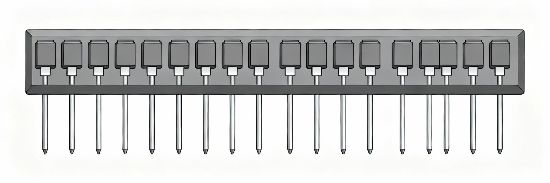
1.1 What the TOMC16031000FT5 is and who makes it
Point: The device is an isolated thin‑film resistor array in an SO‑16 package used in precision analog circuits. Evidence: Common use cases include resistor arrays for sensor conditioning, pull‑up banks, and precision input networks. Explanation: For board designers, its isolated topology removes internal busses, enabling flexible routing and avoiding unintended common nodes in measurement chains.
1.2 Quick spec snapshot (for article lead table)
Point: Compact reference of key specs to guide component selection. Evidence: See table below for typical values engineers verify before layout. Explanation: Keep this table handy when building BOM entries and confirming power and thermal margins during early design reviews.
| Parameter | Typical / Spec |
|---|---|
| Resistance | 100 Ω |
| Tolerance | ±1% |
| Power per element | 100 mW |
| Number of resistors | 8 (isolated) |
| TCR | ±25 ppm/°C |
| Package | SO‑16, 0.220" (5.59 mm) width |
| Pin count | 16 |
Electrical specs & performance analysis
2.1 Key electrical parameters explained
Point: Resistance value, tolerance, element power and TCR define expected behavior. Evidence: A ±1% tolerance and ±25 ppm/°C TCR limit drift and influence matching in multi‑element circuits. Explanation: Designers must factor worst‑case drift (∆R ≈ R·TCR·∆T) into precision gain and divider calculations and ensure element power ratings are not exceeded under ambient and self‑heating conditions.
2.2 Noise, matching, and reliability considerations
Point: Thin‑film networks offer low excess noise and good element‑to‑element matching compared with thick‑film parts. Evidence: Matching plus low TCR reduces gain error and offset drift in ADC front ends. Explanation: For reliability, perform thermal derating: calculate continuous allowable power per element on the PCB considering copper, nearby components, and expected ambient; add margin and test with thermal soak measurements.
PCB footprint & land‑pattern guidance for TOMC16031000FT5
3.1 Recommended SO1116 land pattern and critical dimensions
Point: Accurate pad geometry and courtyard are essential for solderability and inspection. Evidence: Use manufacturer mechanical drawing for pad‑to‑pad pitch, overall length/width, and lead heel dimensions. Explanation: Define pad size to support consistent fillet formation, include solder mask clearance, and mark orientation; verify the TOMC16031000FT5 footprint dimensions against vendor mechanical data before final Gerbers.
3.2 Stencil, solder paste and pick‑and‑place considerations
Point: Stencil aperture and paste volume directly affect wetting and tombstoning risk. Evidence: Typical guidance is 60–80% paste coverage per pad for SO‑16 gull‑wing leads and using a Type 3–4 SN63/Pb‑free paste per assembly spec. Explanation: Center vacuum pickup, set placement tolerance to ±0.1 mm, and inspect fillets post‑reflow; adjust stencil apertures if insufficient solder fillets or tombstoning appear on first runs.
How to read the TOMC16031000FT5 datasheet (step‑by‑step)
4.1 Sections to verify before layout
Point: Key datasheet sections inform layout and procurement decisions. Evidence: Mechanical drawings, electrical characteristics, environmental ratings and packaging notes contain mandatory constraints. Explanation: Confirm measurement conditions (e.g., power per element test conditions) and review moisture sensitivity and tape‑and‑reel details to set handling and storage requirements prior to placing orders.
4.2 Pre‑production checklist (what to confirm before sending Gerbers)
Point: A short validation checklist reduces prototyping rework. Evidence: Verify footprint vs. mechanical drawing, run thermal and power calculations, and order sample reels for initial runs. Explanation: On receipt, spot‑check resistances with a DVM, run a solderability test board, and measure per‑element resistance and TCR on a small population to confirm lot consistency.
Equivalents, alternatives & real‑world use cases
5.1 Cross‑reference and substitute parts
Point: Alternatives exist across thin‑film resistor network families and competing manufacturers. Evidence: When substituting, compare tolerance, TCR, element power, and isolation type. Explanation: A true drop‑in replacement must match pinout, package outline, and electrical parameters; otherwise rework or minor PCB changes may be required to preserve precision performance.
5.2 Application examples and typical circuits
Point: Common applications include pull‑up banks, input termination arrays, and sensor balancing networks near ADC inputs. Evidence: Locating the resistor array close to the sensor or ADC minimizes trace length and parasitic error. Explanation: Place the SO‑16 so that traces to ADC inputs are short and symmetric; place decoupling and reference components nearby to maintain stable measurement nodes.
Actionable design & verification checklist (what to do next)
6.1 Quick PCB design checklist
Point: A concise set of layout and BOM rules speeds review cycles. Evidence: Confirm land‑pattern against vendor drawing, set appropriate stencil, define silkscreen orientation, and document tolerances in the BOM. Explanation: Include full part identifier and packaging in the BOM entry, and specify procurement details so assembly houses source the correct isolated 8‑resistor SO‑16 device and apply proper reflow profiles.
6.2 Prototype test plan and go/no‑go criteria
Point: Define objective tests before approving a build for scale. Evidence: Recommended tests include per‑element resistance verification, thermal soak with applied power, and post‑reflow inspection for opens/shorts. Explanation: Acceptance thresholds: resistances within tolerance bands, no opens/shorts after reflow, and resistance stability consistent with TCR expectations after thermal cycling.
Summary
Use the datasheet to confirm electrical ratings (100 mW per element, ±25 ppm/°C TCR, ±1% tolerance), adhere to the SO‑16 land‑pattern recommendations, and apply the PCB and prototype checklists above. Correct pad geometry, stencil settings, and preproduction verification reduce rework and help ensure first‑pass prototype success for precision resistor array designs.
Key summary
- Confirm land pattern and pad dimensions against the mechanical drawing before generating Gerbers; this prevents solderability and fit issues on the SO‑16 package.
- Verify electrical limits: 100 mW per element and ±25 ppm/°C TCR—use these to calculate drift and safe continuous power on your specific PCB.
- Run prototype tests: per‑element resistance, thermal soak under applied power, and post‑reflow inspection to validate assembly and reliability.
FAQ
Is TOMC16031000FT5 suitable for precision ADC front ends?
Yes. The isolated thin‑film array’s tight tolerance and low TCR make it suitable for ADC front ends when matching and drift are critical; place the array close to the ADC inputs and verify per‑element matching under expected thermal conditions during prototyping.
What PCB footprint checks should I run for the SO‑16 land pattern?
Compare pad‑to‑pad pitch and overall package dimensions to the mechanical drawing, validate pad sizes for consistent fillets, add solder mask dams, and verify courtyard and orientation marks. Run a 3D clearance check in CAD to ensure component fits with nearby parts.
How should I validate TCR and power derating in prototype?
Measure baseline resistance at room temperature, apply controlled power to an element and record resistance after thermal steady state; calculate drift using measured ∆T and compare against the TCR spec. Use that data to set derating margins for reliable continuous operation.
- Technical Features of PMIC DC-DC Switching Regulator TPS54202DDCR
- STM32F030K6T6: A High-Performance Core Component for Embedded Systems
- APT50GH120B Datasheet Deep Dive: Specs, Ratings & Curves
- APT50GH120BSC20 Power Module: Latest Performance Report
- APT50GH120BD30 IGBT: How to Maximize Efficiency for EV Drive
- GTSM20N065: Latest 650V IGBT Test Report & Metrics
- CMSG120N013MDG Performance Report: Efficiency & Losses
- GTSM40N065D Technical Deep Dive: 650V IGBT + SiC SBD
- NOMC110-410UF SO-16: Live Stock & Price Report
- TOMC16031000FT5 Datasheet: Key Specs & Performance
-
 EXB-V4V120JVPanasonic Electronic ComponentsRES ARRAY 2 RES 12 OHM 0606
 -
 EXB-V4V473JVPanasonic Electronic ComponentsRES ARRAY 2 RES 47K OHM 0606
 -
 EXB-V4V823JVPanasonic Electronic ComponentsRES ARRAY 2 RES 82K OHM 0606
 -
 EXB-V4V151JVPanasonic Electronic ComponentsRES ARRAY 2 RES 150 OHM 0606
 -
 EXB-V4V181JVPanasonic Electronic ComponentsRES ARRAY 2 RES 180 OHM 0606
 -
 EXB-V4V331JVPanasonic Electronic ComponentsRES ARRAY 2 RES 330 OHM 0606
 -
 EXB-V4V152JVPanasonic Electronic ComponentsRES ARRAY 2 RES 1.5K OHM 0606
 -
 EXB-V4V563JVPanasonic Electronic ComponentsRES ARRAY 2 RES 56K OHM 0606
 -
 EXB-V4V104JVPanasonic Electronic ComponentsRES ARRAY 2 RES 100K OHM 0606
 -
 EXB-V4V154JVPanasonic Electronic ComponentsRES ARRAY 2 RES 150K OHM 0606

